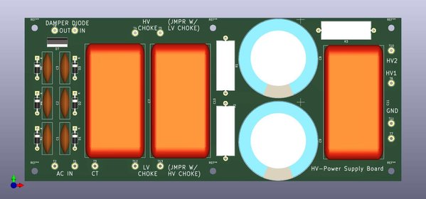
All,
I am starting on a new project updating the pair of 845/211 SET amplifiers that Grover built for Bob Olson back a couple decades ago. The amplifier has had some issues with excessive noise (hum), which has not been solved despite Charlie Phelps and Dave Berning taking a look at it to figure out why they are so noisy. Anyway, I have agreed to take on the task with the current owner to get these quiet, making the construction a bit safer (Grovers' builds at this time were infamous for breadboard construction with flying leads and generous application of RTV silicone applied for insulation from the 950V B+. Not something you want to stick your hands in when running. Also, at the request of the current owner, the amp will be optimized for 211 tubes rather than maintaining 211 and 845 convertibility. The voltage swing for a 211 is much less than for an 845, but it is power limited unless one drives it into A2 operation. Therefore, my approach is to use a single front end tube (D3A or similar) for voltage amplification, with a MOSFET source follower direct coupled to the grid of the 211 to supply grid current as it transitions in to A2 operation. This is the "Power Drive" concept that George at TubeLab advocates, as well as other builders such as Al Moglia as Bartola Valves. The amp would go from a 12W Class A1 to a 30W Class A2 output capability.
I have designed a couple of power supply boards using DC Link capacitors and KEMET high reliability electrolytic capacitors for the 211 SET rebuild project I am working on for Myles Burgess. I am doing the final check on them before sending them out to fabrication, but I have designed the Driver Power supply board to be applicable for other designs up to 600V. Since per board costs in qty are pretty cheap, I can make extras for use in other builds.
A few words about the boards.
The HV board is a CLC circuit for up to 1200V output using a FW rectifier with three (3) stacked UF4007 diodes per side with 0.01uF/1000V bypass caps to ensure equal voltage handling on each diode. Using a series SiC diode at the output of the FW rectifier to prevent any reverse recovery spike on the UF4007 diodes, optionally an offboard damper diode can be used for the same function plus soft start. Included is the provision for offboard power chokes, either on the HV side or the Ground side depending on whether your chokes can take the elevated B+. The DC link capacitors are Vishay 20uF/1200VDC, the two series connected electrolytics are nominally 390uF/600VDC KEMETs (15000 Hr). Of course using voltage equalizing resistors in parallel with the capacitors.
The Driver board is a CLCRC circuit for up to 600V output. Rectifier can be either bridge (no CT) or FW (with CT, omitting two diodes). Again, using UF4007 diodes with SiC or tube damper diode at the output of the rectifiers. Instead of a choke, the pad spacing will accept a power resistor in the first Pi filter. The design uses Panasonic 40uF/600VDC DC link capacitors and KEMET 220uF/600V long life electrolytic caps. There are two DC outputs after each filter stage.
Attached are some pictures of the design, the layout is compact and should fit nicely in a chassis. The boards are designed with the traces on the back side but through-hole pads.
Let me know if you are interested in a few boards. I do not expect the cost to be more than a few $ per board.
David
- Attachments
-
- HV Power Supply Layout.pdf
- (72.69 KiB) Downloaded 1185 times
-

-
